



 Daily Bazar
  Electronics
  Mother, Baby & Toys
  Beauty
  Sports
  Automotive
  Stationery, Books & Music
  Fashion
 _20.jpeg) Home
Home  Garden & Pet Care
  Grocery
  Daily Bazar
  Electronics
  Mother, Baby & Toys
  Beauty
  Sports
  Automotive
  Stationery, Books & Music
  Fashion
 _20.jpeg) Home
Home  Garden & Pet Care
  Grocery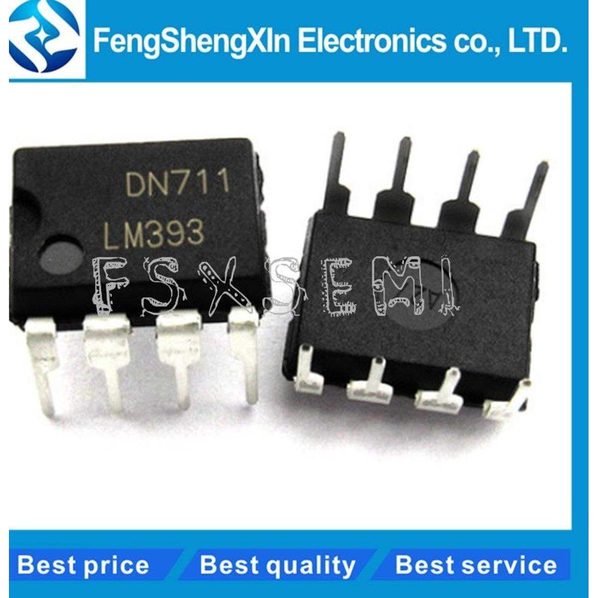
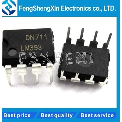
Description: LM393 Low Offset Voltage Dual Comparator IC LM 393 Dual Supply Operation IC DIP 8 Pin IC
The LM393 series are dual independent precision voltage comparators capable of single or split supply operation. These devices are designed to permit a common mode range− to−ground level with single supply operation. Input offset voltage specifications as low as 2.0 mV make this device an excellent selection for many applications in consumer, automotive, and industrial electronics.
LM393 Low Offset Voltage Dual Comparator LM393 is a dual precision voltage comparator IC capable of single or dual supply operation.LM393 IC is designed to permit a common mode range to ground level with single supply operation. Input offset voltage specifications as low as 2.0 mVolt make this device an excellent selection for many applications in consumer, automotive, and industrial electronics.LM393 IC is used in most of the digital comparator Modules that is used in GAS sensor modules, rain sensors etc.
TheLM393ICcan be considered as theequivalent comparatorversion of the most popularLM358 Op-Amp. While any Op-Amp can be made to work as a voltage comparator, the LM393 proves itself to be advantages by providing an open collector output making it suitable to drive loads.
The output transistor can drive loads upto 50V and 50mA which is suitable for driving most of the TTL, MOS and RTL loads. The transistor can also make the Load to be isolated from the system ground. So if you are looking for a Voltage comparator to drive loads of these specifications then this IC might be the right choice for you.
Features:
- Wide Single−Supply Range: 2.0 Vdc to 36 Vdc
- Split−Supply Range: ±1.0 Vdc to ±18 Vdc
- Very Low Current Drain Independent of Supply Voltage: 0.4 mA
- Low Input Bias Current: 25 nA
- Low Input Offset Current: 5.0 nA
- Low Input Offset Voltage: 5.0 mV (max) LM293/393
- Input Common Mode Range to Ground Level
- Differential Input Voltage Range Equal to Power Supply Voltage
- Output Voltage Compatible with DTL, ECL, TTL, MOS, and CMOS Logic Levels
- ESD Clamps on the Inputs Increase the Ruggedness of the Device without Affecting Performance
- NCV Prefix for Automotive and Other Applications Requiring Site and Control Changes
- Pb−Free Packages are Available
Features of LM393 Comparator IC:
- Very Low Current Drain Independent of Supply Voltage 0.4 mA
- Low Input Offset Voltage 5.0 mV (max) LM293/393
- Input Common Mode Range to Ground Level
- Differential Input Voltage Range Equal to Power Supply Voltage
- Output Voltage Compatible with DTL, ECL, TTL, MOS, and CMOS Logic Levels
- These Devices are PbFree, Halogen Free/BFR Free and are RoHS Compliant
LM393 Equivalents
- LM358, TL082,LM311
Alternatives Comparator Op-Amp IC
- LM741,LM358, LM339,LM324
How to use LM393
The LM393 applications arevery similar to theLM311 Comparator IC, only the specifications change a bit. Other than that the LM311 can be considered as a close replacement for LM393. Like all voltage Comparators the LM393 also has an Inverting Pin and a Non-Inverting Pin. If the voltage at the Non-Inverting Terminal (pin 2) is high than the Inverting Terminal (pin 2) the output (pin 7) will also be high else the output will be low.
Let us assume theLM393is powered with the +5V supply voltage circuit since this is the most used design for digital circuits. In this type, the VCC+ (pin 8) is connected to +5V supply voltage and the VCC (pin 4) is grounded to hold it at 0V potential. A sample circuit is shown below in which the Inverting Terminal is set to 2.5V and the Non-Inverting Terminal voltage is varied using a potentiometer. You can note that the Output voltage stays high when pin 2 has higher voltage than pin 7 and vice versa.
The pins 5 and 6 on the Op-amp are used to set the balance voltage if you want to manually adjust the DC-Offset voltage. Normally these pins are not used since the Input Offset itself is much better controlled. When not in use the pins 5 and 6 should be shorted as shown above. You can also notice that the Collector pin (pin 7) of the transistor is used for output and the emitter pin (pin 1) is grounded this type of design is called “Collector output Circuit”, however this does not have to be the case always.
Applications
- Voltage Comparator circuits
- Can drive Relay, Lamp, Motor Etc
- Zero Crossing detector
- Peak voltage Detector
- High Voltage protection/Warning
- Oscillator circuits

Login to ask a question
