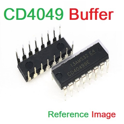
Description: CD4049 Buffer
The CD4049UB and CD4050B devices are inverting and non-inverting hex buffers, respectively, and feature logiclevel conversion using only one supply voltage (VCC). The input-signal high level (VIH) can exceed the VCC supply voltage when these devices are used for logic-level conversions. These devices are intended for use as CMOS to DTL/TTL converters and can drive directly two DTL/TTL loads. (VCC = 5V, VOL £ 0.4V, and IOL ³ 3.3mA.)The CD4049UB and CD4050B are designated as replacements for CD4009UB and CD4010B, respectively.Because the CD4049UB and CD4050B require only one power supply, they are preferred over the CD4009UB and CD4010B and should be used in place of the CD4009UB and CD4010B in all inverter, current driver, or logic-level conversion applications. In these applications the CD4049UB and CD4050B are pin compatible with the CD4009UB and CD4010B respectively, and can be substituted for these devices in existing as well as in new designs. Terminal No. 16 is not connected internally on the CD4049UB or CD4050B, therefore, connection to this terminal is of no consequence to circuit operation. For applications not requiring high sink-current or voltage conversion, the CD4069UB Hex Inverter is recommended.
Features:
- CD4049UB Inverting
- CD4050B Non-Inverting
- High Sink Current for Driving 2 TTL Loads
- High-To-Low Level Logic Conversion
- 100% Tested for Quiescent Current at 20V
- Maximum Input Current of 1mA at 18V Over Full Package Temperature Range; 100nA at 18V and 25oC
- 5V, 10V and 15V Parametric Ratings Applications
- CMOS to DTL/TTL Hex Converter
- CMOS Current “Sink” or “Source” Driver
- CMOS High-To-Low Logic Level Converter
- Voltage Rating:-0.5V to20VDC Input Current, Any One Input:±10mATemperature Range: -55°C to 125°C
Login to ask a question


 Global Finds
  Quick Commerce
  Electronics & Appliances
  Mother, Baby & Toys
  Beauty
  Sports
  Automotive
  Stationery, Books & Music
 _20.png) Fashion Luxe
Fashion Luxe _20.jpeg) Home
Home  Garden & Pet Care
  Special Weekly Offer
  Grocery
  Global Finds
  Quick Commerce
  Electronics & Appliances
  Mother, Baby & Toys
  Beauty
  Sports
  Automotive
  Stationery, Books & Music
 _20.png) Fashion Luxe
Fashion Luxe _20.jpeg) Home
Home  Garden & Pet Care
  Special Weekly Offer
  Grocery


